- 您现在的位置:买卖IC网 > Sheet目录488 > NTGD3133PT1G (ON Semiconductor)MOSFET P-CH DUAL 20V 21.5A 6TSOP
�� �
�
�NTGD3133P�
�Power� MOSFET�
�?� 20� V,� ?� 2.5� A,� P� ?� Channel,� TSOP� ?� 6� Dual�
�Features�
�?�
�?�
�?�
�?�
�?�
�Reduced� Gate� Charge� for� Fast� Switching�
�?� 2.5� V� Gate� Rating�
�Leading� Edge� Trench� Technology� for� Low� On� Resistance�
�Independent� Devices� to� Provide� Design� Flexibility�
�This� is� a� Pb� ?� Free� Device�
�V� (BR)DSS�
�?� 20� V�
�http://onsemi.com�
�R� DS(on)� MAX�
�145� m� W� @� ?� 4.5� V�
�I� D� MAX�
�?� 2.2� A�
�Applications�
�200� m� W� @� ?� 2.5� V�
�?� 1.6� A�
�?�
�?�
�?�
�?�
�Li� ?� Ion� Battery� Charging�
�Load� Switch� /� Power� Switching�
�DC� to� DC� Conversion�
�Portable� Devices� like� PDA’s,� Cellular� Phones,� and� Hard� Drives�
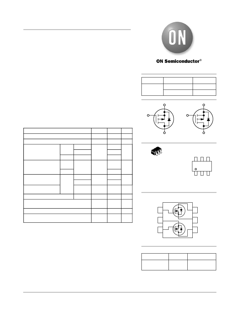
�G1�
�S1�
�G2�
�S2�
�MAXIMUM� RATINGS� (T� J� =� 25� °� C� unless� otherwise� noted)�
�Parameter�
�Drain� ?� to� ?� Source� Voltage�
�Gate� ?� to� ?� Source� Voltage�
�Symbol�
�V� DSS�
�V� GS�
�Value�
�?� 20�
�±� 12�
�Unit�
�V�
�V�
�D1�
�P� ?� CHANNEL� MOSFET�
�D2�
�P� ?� CHANNEL� MOSFET�
�Continuous� Drain�
�Current� (Note� 1)�
�Steady�
�State�
�T� A� =� 25� °� C�
�T� A� =� 85� °� C�
�I� D�
�?� 2.2�
�?� 1.6�
�A�
�MARKING�
�DIAGRAM�
�t� ≤� 5s�
�T� A� =� 25� °� C�
�?� 2.5�
�1�
�SC� =� Specific� Device� Code�
�Power� Dissipation�
�(Note� 1)�
�Continuous� Drain�
�Current� (Note� 2)�
�Power� Dissipation�
�(Note� 2)�
�Pulsed� Drain� Current�
�Steady�
�State�
�t� ≤� 5s�
�Steady�
�State�
�T� A� =� 25� °� C�
�T� A� =� 25� °� C�
�T� A� =� 85� °� C�
�T� A� =� 25� °� C�
�t� p� =� 10� m� s�
�P� D�
�I� D�
�P� D�
�I� DM�
�1.0�
�1.3�
�?� 1.6�
�?� 1.2�
�0.56�
�?� 7.5�
�W�
�A�
�W�
�A�
�TSOP6�
�CASE� 318G� SC� M� G�
�STYLE� 13� G�
�1�
�M� =� Date� Code�
�G� =� Pb� ?� Free� Package�
�(Note:� Microdot� may� be� in� either� location)�
�PIN� CONNECTION�
�Operating� Junction� and� Storage� Temperature�
�T� J� ,� T� STG�
�?� 55� to�
�150�
�°� C�
�Source� Current� (Body� Diode)�
�Lead� Temperature� for� Soldering� Purposes�
�(1/8� ″� from� case� for� 10� s)�
�I� S�
�T� L�
�?� 0.8�
�260�
�A�
�°� C�
�G1�
�S2�
�1�
�2�
�6�
�5�
�D1�
�S1�
�Stresses� exceeding� Maximum� Ratings� may� damage� the� device.� Maximum�
�Ratings� are� stress� ratings� only.� Functional� operation� above� the� Recommended�
�Operating� Conditions� is� not� implied.� Extended� exposure� to� stresses� above� the�
�Recommended� Operating� Conditions� may� affect� device� reliability.�
�G2�
�3�
�4�
�D2�
�1.� Surface� Mounted� on� FR4� Board� using� 1� in� sq� pad� size� (Cu� area� =� 1.127� in� sq�
�[2� oz]� including� traces).�
�2.� Surface� Mounted� on� FR4� Board� using� the� minimum� recommended� pad� size�
�(Cu� area� =� 30� mm� 2� [2� oz]� including� traces).�
�(Top� View)�
�ORDERING� INFORMATION�
�Device�
�NTGD3133PT1G�
�Package�
�TSOP6�
�Shipping� ?�
�3000/Tape� &� Reel�
�(Pb� ?� Free)�
�?For� information� on� tape� and� reel� specifications,�
�including� part� orientation� and� tape� sizes,� please�
�refer� to� our� Tape� and� Reel� Packaging� Specification�
�Brochure,� BRD8011/D.�
�?� Semiconductor� Components� Industries,� LLC,� 2008�
�May,� 2008� ?� Rev.� 1�
�1�
�Publication� Order� Number:�
�NTGD3133P/D�
�发布紧急采购,3分钟左右您将得到回复。
相关PDF资料
NTGD3147FT1G
MOSFET P-CH 20V 2.2A 6-TSOP
NTGD3148NT1G
MOSFET N-CH DUAL 20V 3.5A 6TSOP
NTGD3149CT1G
MOSFET COMPL 20V DUAL 6-TSOP
NTGD4161PT1G
MOSFET P-CH DUAL 30V 2.3A 6-TSOP
NTGD4167CT1G
MOSFET N/P-CH 30V DUAL 6-TSOP
NTGD4169FT1G
MOSFET N-CH 30V 2.6A 6-TSOP
NTGS1135PT1G
MOSFET P-CH 8V 4.6A 6-TSOP
NTGS3130NT1G
MOSFET N-CH SGL 20V 5.6A 6-TSOP
相关代理商/技术参数
NTGD3133PT1H
制造商:Rochester Electronics LLC 功能描述: 制造商:ON Semiconductor 功能描述:
NTGD3147F
制造商:ONSEMI 制造商全称:ON Semiconductor 功能描述:Power MOSFET and Schottky Diode−20 V, −2.5 A, P−Channel with Schottky Barrier Diode, TSOP−6
NTGD3147FT1G
功能描述:MOSFET FETKY 20V 2.5A 145M TSOP6 RoHS:否 制造商:STMicroelectronics 晶体管极性:N-Channel 汲极/源极击穿电压:650 V 闸/源击穿电压:25 V 漏极连续电流:130 A 电阻汲极/源极 RDS(导通):0.014 Ohms 配置:Single 最大工作温度: 安装风格:Through Hole 封装 / 箱体:Max247 封装:Tube
NTGD3148
制造商:ON Semiconductor 功能描述:MOSFET NN CH 20V 3.5A 6TSOP 制造商:ON Semiconductor 功能描述:MOSFET, NN CH, 20V, 3.5A, 6TSOP
NTGD3148N
制造商:ONSEMI 制造商全称:ON Semiconductor 功能描述:Power MOSFET 20 V, 3.5 A, Dual N-Channel, TSOP-6
NTGD3148NT1G
功能描述:MOSFET NFET 20V 3A 70MOHM TSOP6 RoHS:否 制造商:STMicroelectronics 晶体管极性:N-Channel 汲极/源极击穿电压:650 V 闸/源击穿电压:25 V 漏极连续电流:130 A 电阻汲极/源极 RDS(导通):0.014 Ohms 配置:Single 最大工作温度: 安装风格:Through Hole 封装 / 箱体:Max247 封装:Tube
NTGD3149C
制造商:ONSEMI 制造商全称:ON Semiconductor 功能描述:Power MOSFET Complementary, 20 V, +3.5/−2.7 A, TSOP−6 Dual
NTGD3149CT1G
功能描述:MOSFET COMP TSOP6 20V 3A TR RoHS:否 制造商:STMicroelectronics 晶体管极性:N-Channel 汲极/源极击穿电压:650 V 闸/源击穿电压:25 V 漏极连续电流:130 A 电阻汲极/源极 RDS(导通):0.014 Ohms 配置:Single 最大工作温度: 安装风格:Through Hole 封装 / 箱体:Max247 封装:Tube